- 您现在的位置:买卖IC网 > Sheet目录1997 > ICS841602AGILF (IDT, Integrated Device Technology Inc)IC CLOCK GENERATOR 28-TSSOP
IDT / ICS HCSL CLOCK GENERATOR
8
ICS841602AGI REV. A JULY 10, 2008
ICS841602I
FEMTOCLOCKS CRYSTAL-TO-HCSL CLOCK GENERATOR
APPLICATION INFORMATION
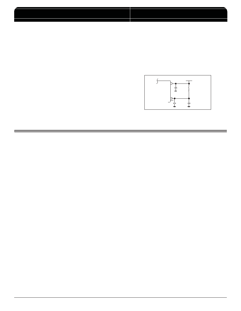
As in any high speed analog circuitry, the power supply pins
are vulnerable to random noise. To achieve optimum jitter
performance, power supply isolation is required. The ICS841602I
provides separate power supplies to isolate any high switching
noise from the outputs to the internal PLL. V
DD and VDDA
should
be individually connected to the power supply plane through
vias, and 0.01F bypass capacitors should be used for each
pin.
Figure 1 illustrates this for a generic V
DD pin and also shows
that V
DDA requires that an additional10Ω resistor along with a
10F bypass capacitor be connected to the V
DDA pin.
POWER SUPPLY FILTERING TECHNIQUES
FIGURE 1. POWER SUPPLY FILTERING
10
Ω
V
DDA
10
μF
.01
μF
3.3V
.01
μF
V
DD
INPUTS:
CRYSTAL INPUTS
For applications not requiring the use of the crystal oscillator input,
both XTAL_IN and XTAL_OUT can be left floating. Though not
required, but for additional protection, a 1k
Ω resistor can be tied
from XTAL_IN to ground.
REF_IN INPUT
For applications not requiring the use of the reference clock,
it can be left floating. Though not required, but for additional
protection, a 1k
Ω resistor can be tied from the REF_IN to ground.
LVCMOS CONTROL PINS
All control pins have internal pull-downs; additional resistance is
not required but can be added for additional protection. A 1k
Ω
resistor can be used.
RECOMMENDATIONS FOR UNUSED INPUT AND OUTPUT PINS
OUTPUTS:
DIFFERENTIAL OUTPUTs
All unused differential outputs can be left floating. We recommend
that there is no trace attached. Both sides of the differential output
pair should either be left floating or terminated.
发布紧急采购,3分钟左右您将得到回复。
相关PDF资料
ICS841608AKI
IC CLOCK GENERATOR 32-VFQFPN
ICS841S012DKILF
IC FREQ SYNTHESIZER 56VFQFN
ICS842023BGLF
IC CLK GEN ETHERNET 25MHZ 8TSSOP
ICS8421002AGILF
IC FREQ SYNTHESIZER 20-TSSOP
ICS8422002AGILF
IC SYNTHESIZER LVHSTL 20-TSSOP
ICS8427DY-02LF
IC SYNTHESIZER 500MHZ 32-LQFP
ICS843001AG-123LF
IC SYNTHESIZER LVPECL 8-TSSOP
ICS843001AG-21LFT
IC SYNTHESIZER LVPECL 24-TSSOP
相关代理商/技术参数
ICS841602AGILFT
功能描述:IC CLOCK GENERATOR 28-TSSOP RoHS:是 类别:集成电路 (IC) >> 时钟/计时 - 时钟发生器,PLL,频率合成器 系列:HiPerClockS™, FemtoClock™ 标准包装:1,000 系列:- 类型:时钟/频率合成器,扇出分配 PLL:- 输入:- 输出:- 电路数:- 比率 - 输入:输出:- 差分 - 输入:输出:- 频率 - 最大:- 除法器/乘法器:- 电源电压:- 工作温度:- 安装类型:表面贴装 封装/外壳:56-VFQFN 裸露焊盘 供应商设备封装:56-VFQFP-EP(8x8) 包装:带卷 (TR) 其它名称:844S012AKI-01LFT
ICS841604AGILF
功能描述:IC CLOCK GENERATOR 28-TSSOP RoHS:是 类别:集成电路 (IC) >> 时钟/计时 - 时钟发生器,PLL,频率合成器 系列:HiPerClockS™, FemtoClock™ 标准包装:2,000 系列:- 类型:PLL 频率合成器 PLL:是 输入:晶体 输出:时钟 电路数:1 比率 - 输入:输出:1:1 差分 - 输入:输出:无/无 频率 - 最大:1GHz 除法器/乘法器:是/无 电源电压:4.5 V ~ 5.5 V 工作温度:-20°C ~ 85°C 安装类型:表面贴装 封装/外壳:16-LSSOP(0.175",4.40mm 宽) 供应商设备封装:16-SSOP 包装:带卷 (TR) 其它名称:NJW1504V-TE1-NDNJW1504V-TE1TR
ICS841604AGILFT
功能描述:IC CLOCK GENERATOR 28-TSSOP RoHS:是 类别:集成电路 (IC) >> 时钟/计时 - 时钟发生器,PLL,频率合成器 系列:HiPerClockS™, FemtoClock™ 标准包装:1,000 系列:- 类型:时钟/频率合成器,扇出分配 PLL:- 输入:- 输出:- 电路数:- 比率 - 输入:输出:- 差分 - 输入:输出:- 频率 - 最大:- 除法器/乘法器:- 电源电压:- 工作温度:- 安装类型:表面贴装 封装/外壳:56-VFQFN 裸露焊盘 供应商设备封装:56-VFQFP-EP(8x8) 包装:带卷 (TR) 其它名称:844S012AKI-01LFT
ICS841608AKI
功能描述:IC CLOCK GENERATOR 32-VFQFPN RoHS:否 类别:集成电路 (IC) >> 时钟/计时 - 时钟发生器,PLL,频率合成器 系列:HiPerClockS™, FemtoClock™ 标准包装:1,000 系列:- 类型:时钟/频率合成器,扇出分配 PLL:- 输入:- 输出:- 电路数:- 比率 - 输入:输出:- 差分 - 输入:输出:- 频率 - 最大:- 除法器/乘法器:- 电源电压:- 工作温度:- 安装类型:表面贴装 封装/外壳:56-VFQFN 裸露焊盘 供应商设备封装:56-VFQFP-EP(8x8) 包装:带卷 (TR) 其它名称:844S012AKI-01LFT
ICS841608AKILF
功能描述:IC CLOCK GENERATOR 32VFQFPN RoHS:是 类别:集成电路 (IC) >> 时钟/计时 - 时钟发生器,PLL,频率合成器 系列:HiPerClockS™, FemtoClock™ 标准包装:2,000 系列:- 类型:PLL 频率合成器 PLL:是 输入:晶体 输出:时钟 电路数:1 比率 - 输入:输出:1:1 差分 - 输入:输出:无/无 频率 - 最大:1GHz 除法器/乘法器:是/无 电源电压:4.5 V ~ 5.5 V 工作温度:-20°C ~ 85°C 安装类型:表面贴装 封装/外壳:16-LSSOP(0.175",4.40mm 宽) 供应商设备封装:16-SSOP 包装:带卷 (TR) 其它名称:NJW1504V-TE1-NDNJW1504V-TE1TR
ICS841608AKILFT
功能描述:IC CLOCK GENERATOR 32-VFQFPN RoHS:是 类别:集成电路 (IC) >> 时钟/计时 - 时钟发生器,PLL,频率合成器 系列:HiPerClockS™, FemtoClock™ 标准包装:1,000 系列:- 类型:时钟/频率合成器,扇出分配 PLL:- 输入:- 输出:- 电路数:- 比率 - 输入:输出:- 差分 - 输入:输出:- 频率 - 最大:- 除法器/乘法器:- 电源电压:- 工作温度:- 安装类型:表面贴装 封装/外壳:56-VFQFN 裸露焊盘 供应商设备封装:56-VFQFP-EP(8x8) 包装:带卷 (TR) 其它名称:844S012AKI-01LFT
ICS841608AKIT
功能描述:IC CLOCK GENERATOR 32-VFQFPN RoHS:否 类别:集成电路 (IC) >> 时钟/计时 - 时钟发生器,PLL,频率合成器 系列:HiPerClockS™, FemtoClock™ 标准包装:1,000 系列:- 类型:时钟/频率合成器,扇出分配 PLL:- 输入:- 输出:- 电路数:- 比率 - 输入:输出:- 差分 - 输入:输出:- 频率 - 最大:- 除法器/乘法器:- 电源电压:- 工作温度:- 安装类型:表面贴装 封装/外壳:56-VFQFN 裸露焊盘 供应商设备封装:56-VFQFP-EP(8x8) 包装:带卷 (TR) 其它名称:844S012AKI-01LFT
ICS841608I
制造商:IDT 制造商全称:Integrated Device Technology 功能描述:FEMTOCLOCKS CRYSTAL-TO-HCSL CLOCK GENERATOR VCO: 500MHz